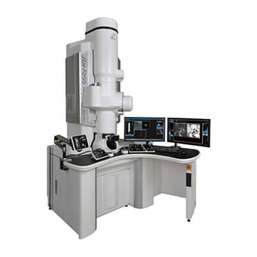
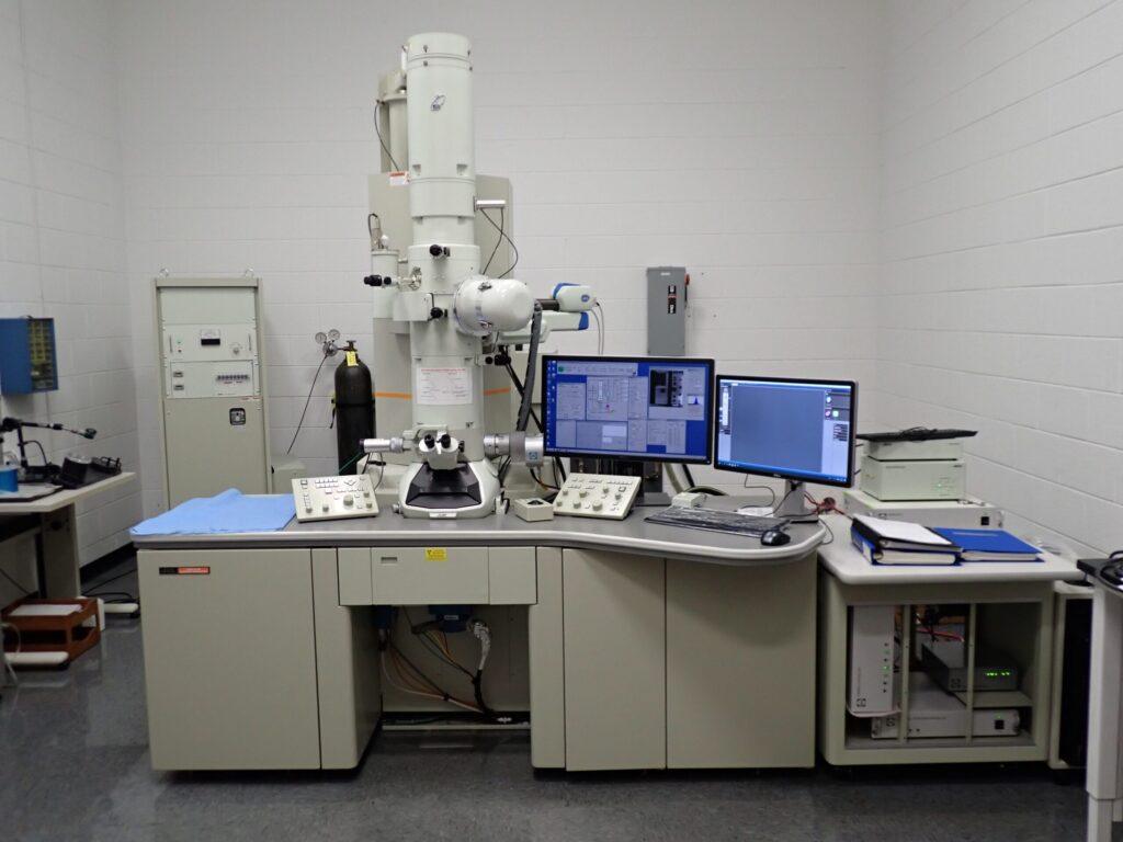
Transmission Electron Microscopy (TEM)
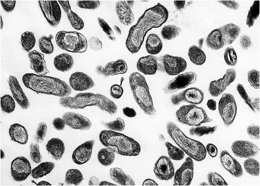
Transmission Electron Microscopy (TEM) is an ultra-high-resolution imaging technique that uses a focused beam of electrons transmitted through an ultrathin specimen. As electrons interact with the sample, they produce contrast based on thickness, density, and atomic composition, allowing visualization of atomic-scale structures, nanoparticles, crystallographic features, and internal microarchitecture.
TEM provides magnifications up to millions of times, making it one of the most powerful imaging tools available for material and biological research.
Use of Transmission Electron Microscopy
TEM is used to analyze internal material structure, crystallinity, and nanoscale features not visible with SEM or optical microscopy.
It enables researchers to:
- Visualize nanoparticles, nanofibers, and molecular assemblies
- Evaluate crystallinity, lattice defects, and grain boundaries
- Inspect internal layers, interfaces, and thin-film structures
- Analyze polymer nanocomposites and filler dispersion
- Characterize biological ultrastructure (post-fixation and sectioning)
- Generate electron diffraction patterns to determine atomic arrangements
Applications of TEM
• Nanomaterials: size, morphology, lattice fringes, crystallographic defects
• Polymers & Composites: nanoparticle dispersion, interphase characterization
• Metals & Ceramics: dislocations, grain boundaries, phase identification
• Thin Films & Coatings: layer thickness, interface quality, nanostructure
• Energy Materials: battery cathode/anode microstructure, nanoparticle clustering
• Biological Samples: cellular ultrastructure (after resin embedding)
Sample Analysis Process
1. Sample Submission & Objective Review
- Provide sample type, imaging goals, and structural details of interest
• Determine whether ultrathin sectioning or nanoparticle drop-casting is required
2. Sample Preparation
TEM requires preparation of electron-transparent samples:
• Ultramicrotomy: slicing resin-embedded materials or biological samples
• Drop-casting: nanoparticles dispersed onto TEM grids
• FIB-thinned lamellae (if needed for site-specific analysis)
• Staining (for biology): uranyl acetate, lead citrate as appropriate
3. TEM Imaging & Diffraction
- Brightfield and darkfield imaging
• High-resolution TEM (HRTEM)
• Electron diffraction (SAED)
• Imaging at multiple accelerating voltages based on sample type
4. Data Processing & Reporting
• High-resolution images with scale bars and lattice measurements
• Particle size distributions
• Crystallographic interpretations (if applicable)
• Annotated report summarizing findings
Why Choose Materials Metric for Your TEM Analysis
Materials Metric provides ultra-high-resolution TEM imaging and nanoscale structural analysis supported by scientific expertise in polymers, nanomaterials, ceramics, and biological systems.
Our TEM services offer:
- High-resolution visualization of nanoparticles and internal microstructures
• Lattice fringe imaging and crystallographic analysis
• Layer/interface characterization for films and coatings
• Accurate particle size and dispersion measurements
• Specialized sample preparation options for diverse materials
• Detailed, annotated reports tailored to your research goals
TEM data can be complemented with XRD, SEM, AFM, spectroscopy, and mechanical/thermal characterization for full structure–property evaluation.