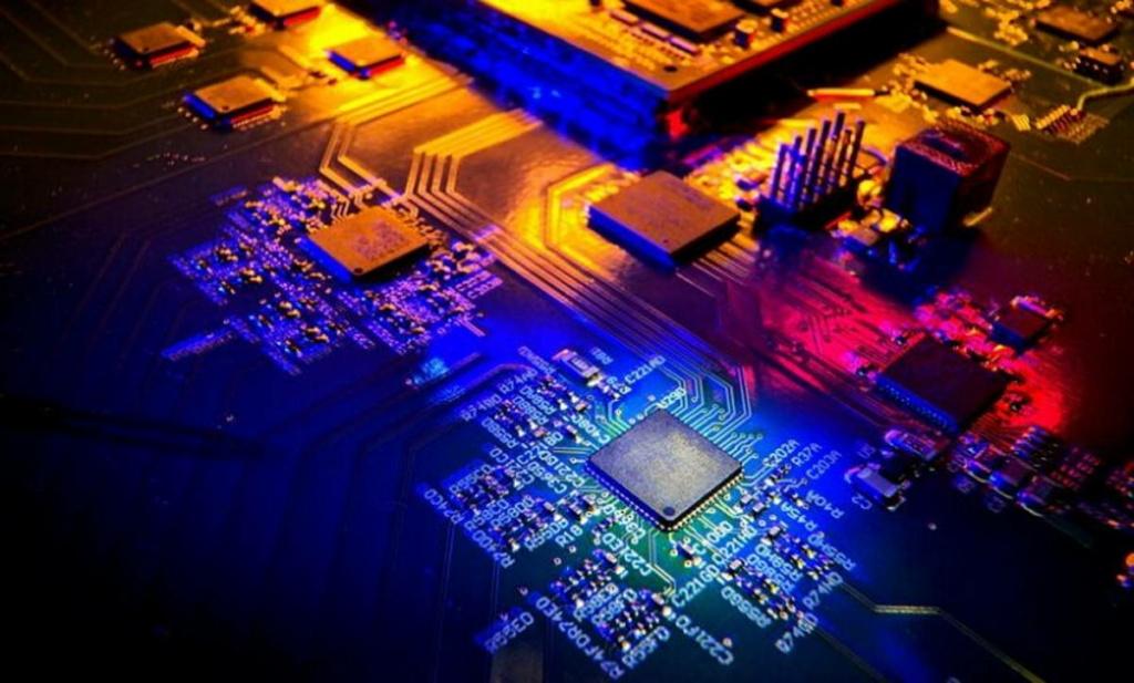
Semiconductor materials testing is a critical foundation of the electronics and microelectronics industry. As devices become smaller, faster, and more complex, the performance and reliability of semiconductor materials must be validated with extreme precision. From wafer fabrication to advanced packaging, materials testing ensures that semiconductor devices meet stringent electrical, thermal, mechanical, and chemical requirements.
Materials Metric supports semiconductor innovation by delivering advanced materials testing, characterization, and data-driven insights tailored to the evolving needs of semiconductor manufacturers, startups, and R&D teams.
Why Materials Testing Is Essential for Semiconductor Devices
Semiconductor devices operate at the limits of material performance. Even minor defects or impurities can lead to device failure, yield loss, or long-term reliability issues. Materials testing provides the data needed to identify these risks early and guide design and process optimization.
Key reasons materials testing is essential in the semiconductor industry include:
Ensuring device reliability and long-term performance
Detecting defects, impurities, and microstructural inconsistencies
Supporting compliance with industry and customer specifications
Reducing costly manufacturing errors and yield loss
Enabling innovation in next-generation semiconductor technologies
Without rigorous testing, manufacturers risk performance degradation, shortened device lifetimes, and reputational damage.
Key Semiconductor Materials and Performance Considerations
Semiconductor performance is fundamentally determined by material selection. Each material offers unique electrical, thermal, and mechanical properties suited to specific applications.
Common semiconductor materials include:
Silicon (Si): The backbone of modern electronics due to its stability, availability, and well-understood properties
Gallium Arsenide (GaAs): Used in high-speed and optoelectronic applications
Silicon Carbide (SiC): Ideal for high-power and high-temperature environments
Gallium Nitride (GaN): Enables high-frequency and high-efficiency power devices
Critical material properties evaluated through testing include:
Electrical conductivity and resistivity
Thermal stability and heat dissipation
Crystallinity and defect density
Band gap and electronic structure
Mechanical integrity and stress tolerance
Accurate characterization of these properties is essential for optimizing device design and manufacturing processes.
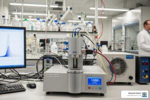
Common Materials Testing Methods in the Semiconductor Industry
Semiconductor materials testing relies on a combination of mechanical, thermal, electrical, and chemical analysis techniques to fully evaluate material behavior.
Mechanical Testing
Evaluates strength, fracture resistance, and durability, particularly important for thin films, wafers, and packaging materials.
Thermal Testing
Measures thermal conductivity, thermal expansion, and heat resistance to ensure device stability under operating conditions.
Electrical Testing
Assesses resistivity, capacitance, and dielectric properties critical for device functionality.
Chemical Analysis
Identifies impurities, contaminants, and compositional variations using techniques such as spectroscopy and chromatography.
Widely used characterization methods include:
X-ray Diffraction (XRD): Determines crystalline structure and phase composition
Scanning Electron Microscopy (SEM): Provides high-resolution surface and microstructural analysis
Together, these techniques form the backbone of semiconductor quality control and failure prevention.
Advanced Characterization Techniques for Semiconductor Materials
As device dimensions shrink and material systems become more complex, advanced characterization techniques are increasingly required.
Key advanced techniques include:
Transmission Electron Microscopy (TEM): Atomic-scale imaging of defects, interfaces, and crystal structure
Atomic Force Microscopy (AFM): Nanoscale surface roughness and topography analysis
Raman Spectroscopy: Non-destructive evaluation of molecular structure, stress, and composition
These methods provide deep insight into material behavior that cannot be captured through conventional testing alone, enabling innovation in next-generation semiconductor devices.
Challenges in Modern Semiconductor Materials Testing
Materials testing for modern semiconductors faces growing technical challenges:
Miniaturization: Detecting defects at nanometer scales
Material Diversity: Testing novel materials with unique properties
Environmental Sensitivity: Managing temperature, humidity, and contamination effects
Complex Device Architectures: Multilayer and heterogeneous material systems
Overcoming these challenges requires advanced instrumentation, custom testing protocols, and robust data analysis.
The Role of Data and Analytics in Semiconductor Materials Testing
Data and analytics play a central role in modern semiconductor materials testing. Each test generates large volumes of complex data that must be processed accurately and efficiently.
Data-driven testing supports:
Defect detection and root-cause analysis
Understanding material behavior under varied conditions
Process optimization and yield improvement
Predictive insights for reliability and performance
Advanced analytics transform raw measurements into actionable insights, enabling faster, more confident decision-making across R&D and manufacturing workflows.
How Materials Metric Supports Semiconductor Materials Testing
Materials Metric provides specialized support for semiconductor materials testing through advanced characterization, custom testing workflows, and data-driven analysis.
Our capabilities include:
Advanced materials characterization for semiconductor substrates, thin films, and coatings
Custom testing protocols aligned with specific device and process requirements
Integrated data analysis to support faster interpretation and reporting
Flexible workflows adaptable to R&D, pilot-scale, and production-stage needs
Materials Metric works closely with clients to translate complex testing challenges into reliable, decision-ready data, supporting yield improvement, reliability assurance, and innovation.
Future Trends in Semiconductor Materials Testing
The future of semiconductor materials testing is shaped by increasing complexity and the demand for faster innovation.
Key trends include:
Greater integration of automation and robotics in testing workflows
Use of artificial intelligence and machine learning for defect detection and data interpretation
Development of testing strategies for emerging semiconductor materials
Real-time and in-line materials characterization
As semiconductor technologies evolve, materials testing will continue to play a central role in enabling progress.
Conclusion: Advancing Semiconductor Innovation Through Materials Testing
Materials testing is indispensable to the success of the semiconductor industry. It ensures device reliability, supports innovation, and reduces manufacturing risk in an increasingly demanding technological landscape.
By combining advanced analytical techniques, custom testing strategies, and data-driven insights, Materials Metric supports semiconductor manufacturers and researchers in developing high-performance, reliable devices. As the industry moves forward, precise and adaptable materials testing will remain a cornerstone of semiconductor innovation.