Scanning Electron Microscopy (SEM)
Scanning Electron Microscopy (SEM) is a high-resolution imaging technique that uses a focused electron beam to scan the surface of a specimen. When electrons interact with the atoms of the material, they produce secondary and backscattered signals that are collected to generate detailed images of surface topography and composition.
Compared to optical microscopy, SEM offers far greater magnification (up to 100,000×) and depth of field, allowing visualization of nanoscale features with exceptional clarity. With integrated Energy Dispersive X-ray Spectroscopy (EDS), SEM also enables elemental identification of regions of interest.
Use of Scanning Electron Microscopy
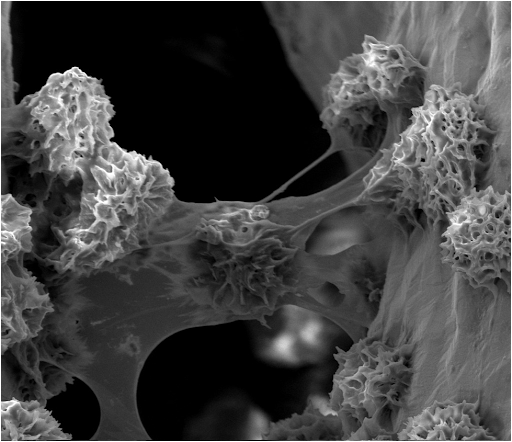
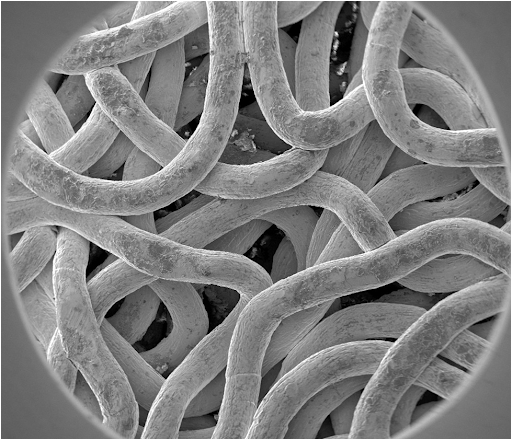
SEM is used to study a material’s surface morphology, microstructure, and elemental composition. It provides both qualitative and quantitative data that help evaluate manufacturing quality, identify defects, and understand performance mechanisms.
Common analytical goals include:
- Characterizing coatings, films, and composites for surface integrity and layer uniformity.
- Performing failure and fracture analysis to determine crack propagation or delamination.
- Mapping particle size and distribution for powders, fillers, or nanomaterials.
- Conducting elemental analysis through EDS for contamination, inclusions, or composition validation.
- Correlating surface texture and processing parameters for product optimization.
Applications of SEM
SEM supports research and development across multiple industries:
- Medical Devices & Biomaterials: Evaluation of implant surfaces, bioactive coatings, and tissue-scaffold integration.
- Polymers & Composites: Fiber dispersion, filler morphology, fracture surfaces, and adhesion quality.
- Metals & Ceramics: Grain structure, corrosion, inclusions, and oxidation studies.
- Electronics & Energy Materials: Inspection of solder joints, cathode/anode microstructure, and failure zones.
- Additive Manufacturing: Porosity, surface roughness, and layer bonding assessment.
Sample Analysis Process
Our SEM analysis workflow ensures high-quality imaging and reproducible results.
1. Sample Submission & Review
- Client provides sample details, objectives, and desired magnification range.
- We evaluate sample type (polymer, metal, ceramic, biological, coating, powder) to determine optimal preparation.
2. Sample Preparation
Depending on material type and conductivity:
- Mounting: samples are secured on SEM stubs using conductive carbon tape.
- Coating (if needed): non-conductive samples may be coated with Au/Pd or carbon to prevent charging.
- Cross-sectioning: materials requiring interface or layered imaging are sectioned and polished.
- Low-vacuum options: available for soft, wet, or uncoated materials.
3. SEM Imaging & EDS Analysis
- Secondary and backscattered electron imaging for morphology and contrast
- High-magnification imaging for nanoscale details
- EDS point, line, or area mapping for elemental analysis
- Optional tilt/rotation for 3D visualization of topography
4. Data Processing & Reporting
- Images provided with scale bars and metadata
- EDS spectra, elemental maps, and quantification (if applicable)
- Annotated analysis report summarizing key findings aligned with your objectives
Why Choose Materials Metric for Your SEM Analysis
At Materials Metric, our SEM analysis service provides nanometer-scale surface imaging and compositional analysis using state-of-the-art instrumentation equipped with secondary, backscattered, and EDS detectors.
Our team of materials scientists and engineers has experience across polymers, biomaterials, metals, and composites, enabling precise interpretation of microstructural data.
We offer:
- High-resolution imaging and EDS elemental mapping for surface and subsurface characterization.
- Cross-sectional and fracture surface analysis for coatings, thin films, and multilayer systems.
- Quantitative image analysis for particle morphology, coating thickness, and surface roughness.
- Custom sample preparation, including sputter coating, low-vacuum imaging, and cryo-SEM for sensitive samples.
- Detailed reporting with annotated images, EDS spectra, and recommendations for next-step validation.
By integrating SEM results with our spectroscopic, mechanical, and thermal testing capabilities, we help clients establish clear structure–property relationships that guide product design and failure prevention.